


.png)


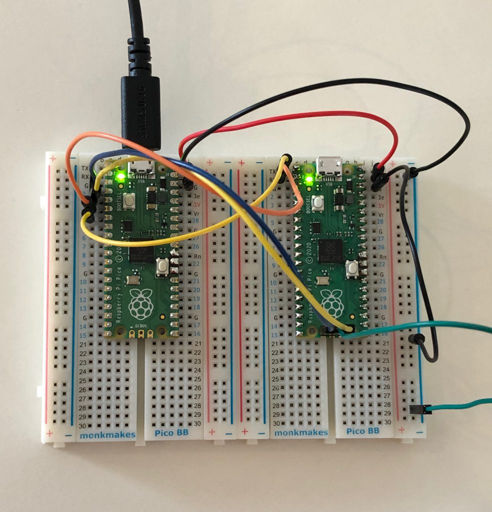
Shipped this project!
final week of LOCK- IN
This is the last ship of Flavortown, there will be updates in the repo after this.
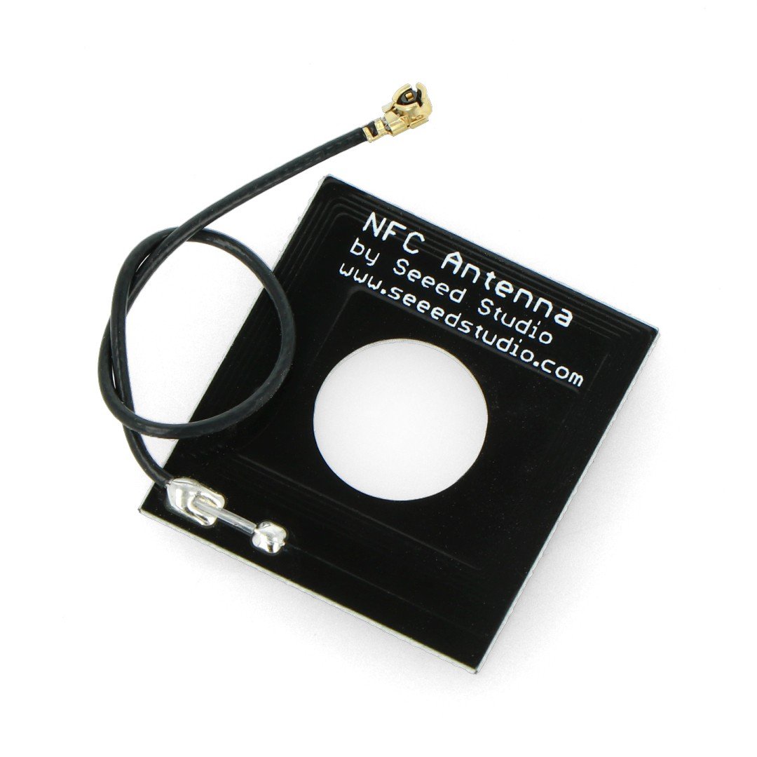
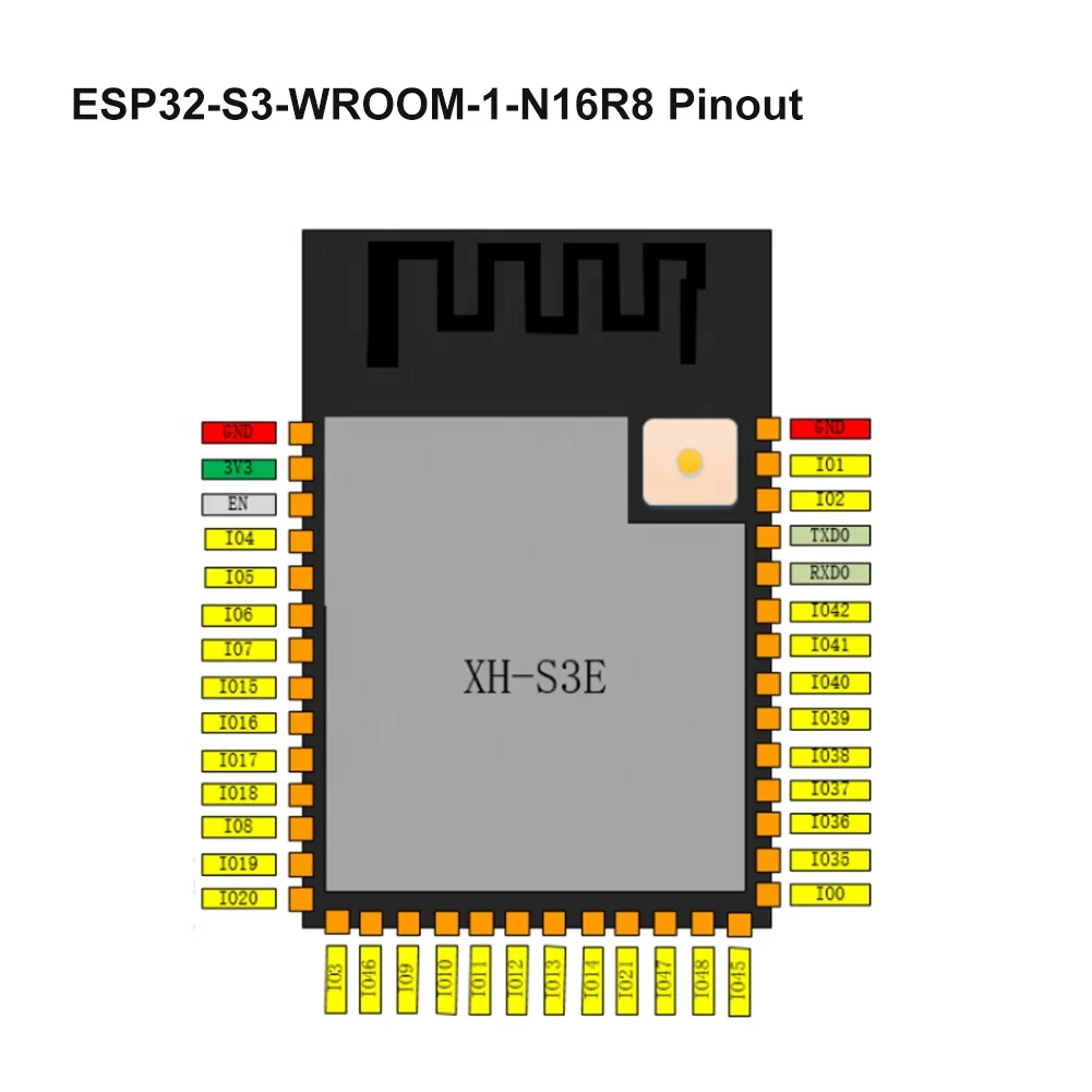
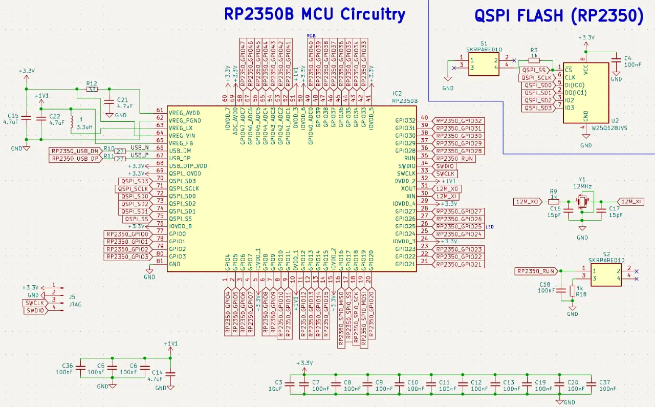
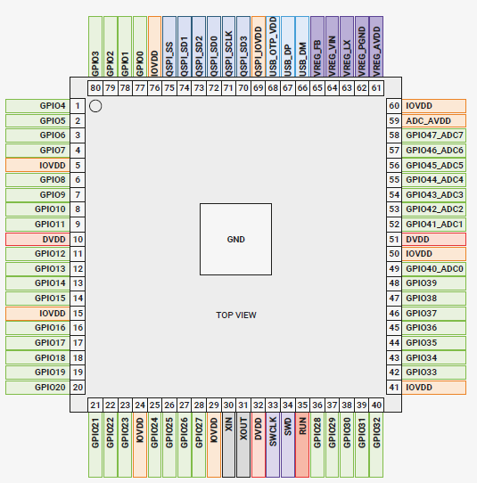
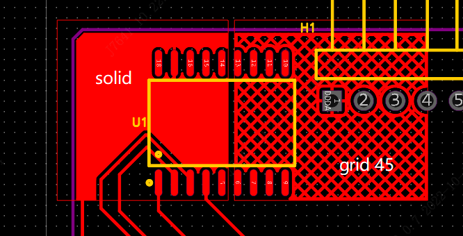
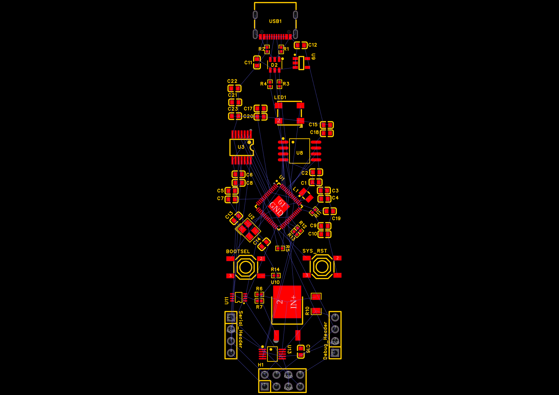
Cyrus is an open-source, highly secure, off-grid communication terminal. Built around the ESP32-S3, it combines long-range RF capabilities (LoRa), precise global positioning (GPS), and secure near-field authentication (NFC) into a portable, pager-like form factor. It is designed for resilient communication environments, featuring both USB-C fast charging and solar energy harvesting.
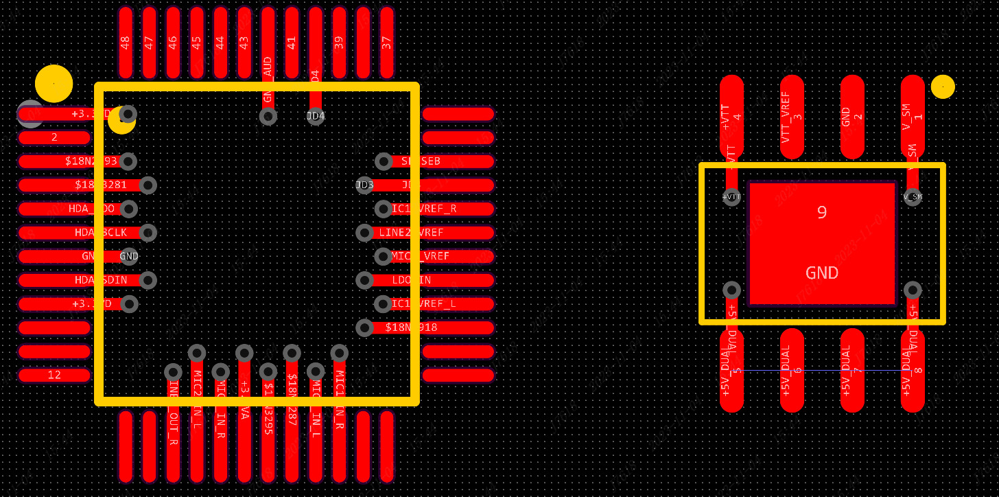
For location awareness and asset tracking, Cyrus features an integrated u-blox GNSS receiver.
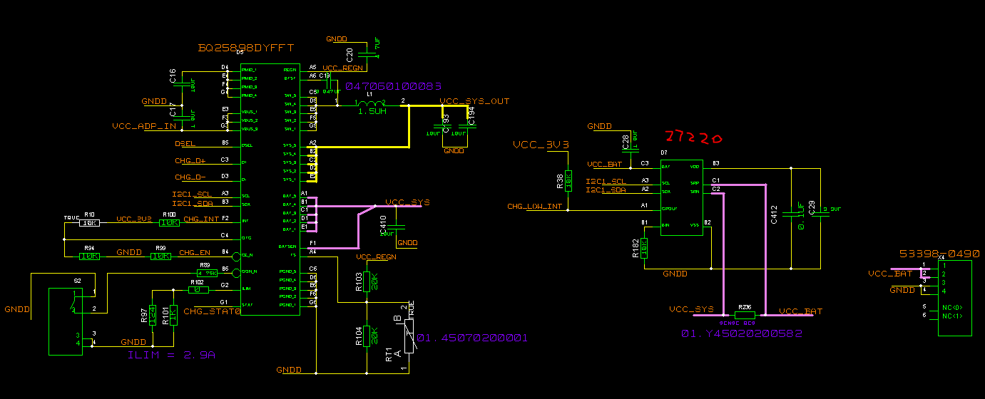
The hardware is designed for indefinite deployment in remote environments. It utilizes a dedicated Maximum Power Point Tracking (MPPT) charge controller to efficiently harvest energy from a 6V solar panel
for all the devlogs please visit the project page (hope you all enjoy it!)


 )
)


 ,
,


.png)


