48 devlogs
87h 36m 6s
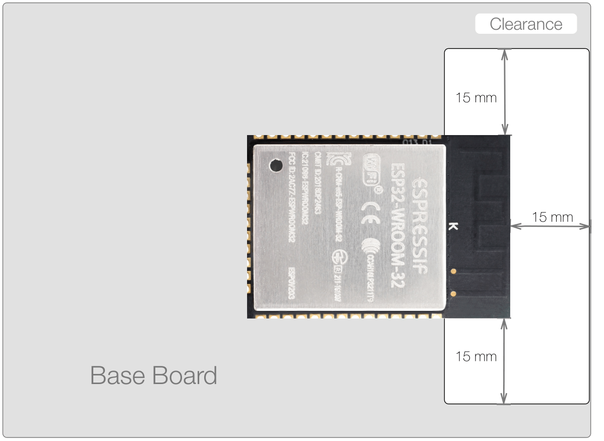
Cyrus is a project allows the use of affordable LoRa radios for long-range, off-grid communication where reliable infrastructure is absent. It is entirely community-driven. it uses the LoRa protocol, which is license-free and widely available in m…
Cyrus is a project allows the use of affordable LoRa radios for long-range, off-grid communication where reliable infrastructure is absent. It is entirely community-driven. it uses the LoRa protocol, which is license-free and widely available in most areas without needing any additional licenses or certifications.unlike HAM radio.
- Ultra-Low-Power GPS Tracking
- Long-Range LoRa Communication: Integrated the Ai-Thinker RA-01SH-P (SX1262) module.
- Continuous Off-Grid Solar Power (6 V solar panel )
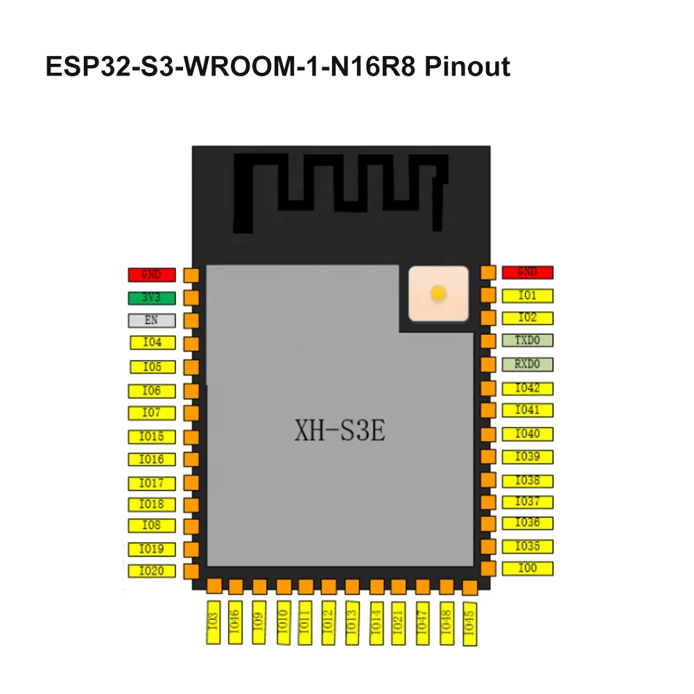
- ESP32_s3 power McU
for more check readme file