PICO debugger  banner

PICO debugger

13 devlogs
18h 17m 1s

The PICO debugger Probe is a custom-built tool to help you fix broken code and test custom electronics boards, that not only debugs your code but also protects your computer from electrical spikes, adapts to any voltage, and tells you exactly ho…

The PICO debugger Probe is a custom-built tool to help you fix broken code and test custom electronics boards, that not only debugs your code but also protects your computer from electrical spikes, adapts to any voltage, and tells you exactly how much power your project is consuming.

I accidentally crashed my Raspberry Pico debugger due to a voltage spike.
standard debuggers only operate at 3.3 volts—if you accidentally plug them into a 5-volt board, you fry your debugger , And that’s exactly what happened to me too
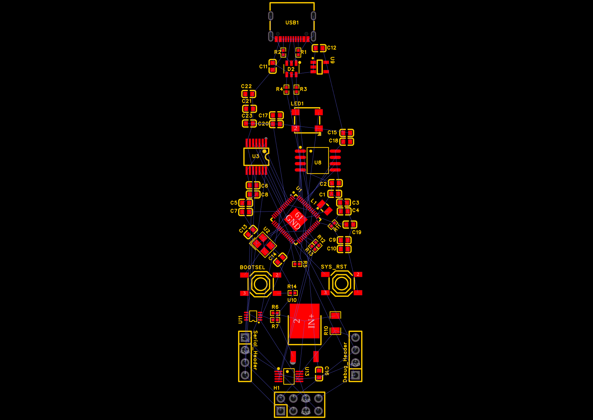
hardwere used :-

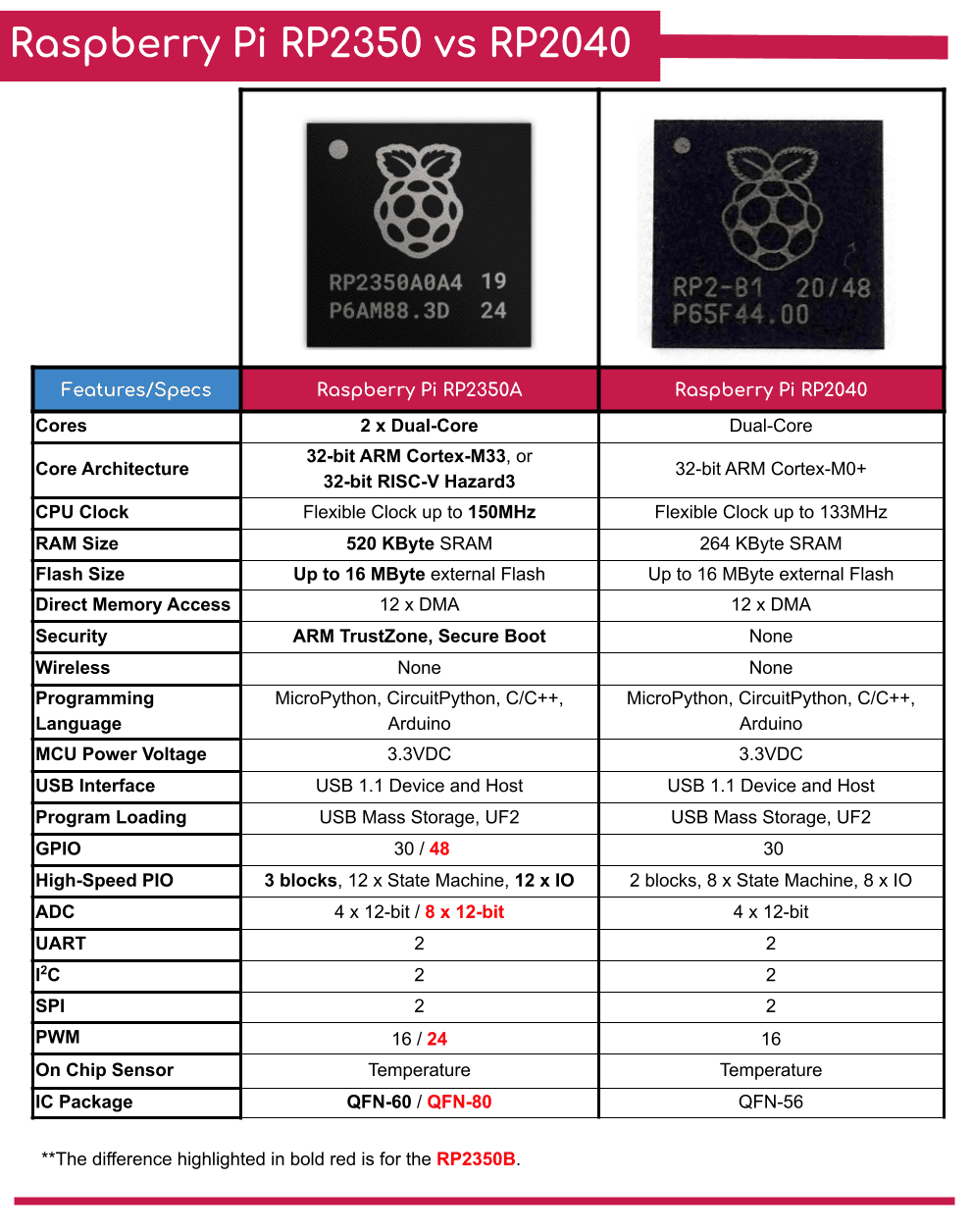
  • Microcontroller: Raspberry Pi RP2350A (QFN-60)
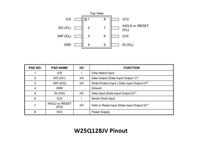
  • Memory: 16MB QSPI Flash (Winbond W25Q128JV)
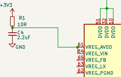
  • Core Power: Custom Switched-Mode Power Supply (SMPS) utilizing a 3.3µH inductor.
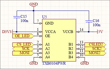
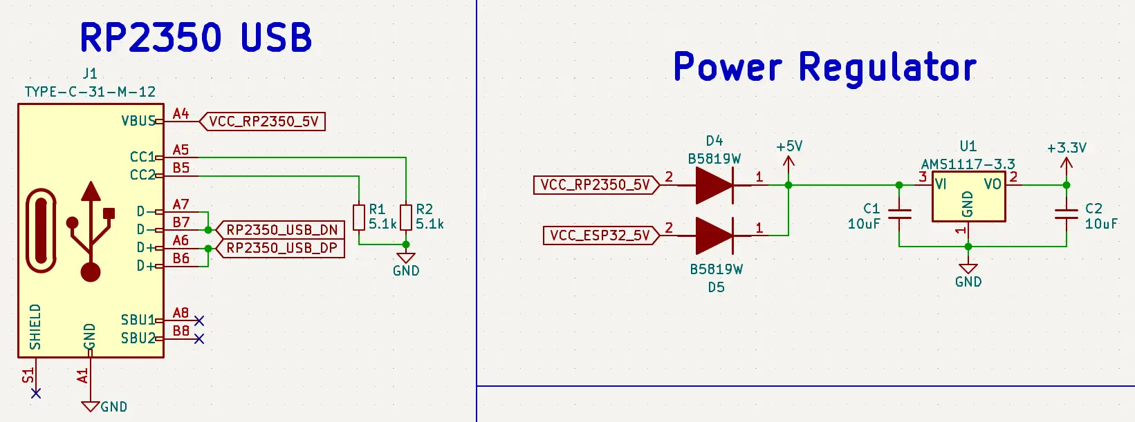
  • logic Level Shifting: * TXB0104 (4-Channel Auto-Direction) for SWD and UART.
    • GT74LVC2T45 (Direction-locked) for Target Hardware Reset.
Demo Repository

Loading README...

ego

I finally have my PCB routing complete, just a few DRC checks left to sort out.

  • I’ll have to redesign half of my PCB because I overlooked differential impedance previously.
  • When designing, you have to worry about high-speed lines where vias aren’t allowed.
  • Every time a high-speed signal changes layers through a via, it changes impedance and can reflect the signal back at the source.
  • By keeping them all on the Top Layer, the signals remain perfectly clean.
Attachment
0
ego

USB 2.0 full-speed signals operate at 12 Mbps ( dont know where i read it lol ) i have to re roaute every thing i am feeling sad.

  • With power and USB handled, I moved to the RP2350’s external memory.
  • The chip boots and runs code directly from the W25Q128JV QSPI flash memory.
  • This interface runs incredibly fast (up to 133 MHz), meaning trace length and signal integrity are vital.
  • I routed all six lines (QSPI_SS, QSPI_CLK, and the four QSPI_SD data lines) exclusively on the Top Layer.
  • I roughly length-matched these traces. It doesn’t require millimeter-perfect meandering like a PC motherboard’s RAM

Attachment
0
ego

started routing the hardest traces first:

  • the USB data lines
  • the RP2350’s internal switching power supply (SMPS).

alt text
For the SMPS, the datasheet is incredibly strict. I placed the 3.3µH inductor on the top layer right next to the VREG_LX and VREG_FB pins.
alt text

  • The switching node (VREG_LX) generates a lot of electrical noise,
  • so I made that copper trace as short and fat as physically possible.
  • I tied the 4.7µF filtering capacitors directly to the output of the inductor
  • USB 2.0 requires the D+ and D- lines to have a differential impedance of 90 ohms
  • I routed these traces together perfectly parallel, avoiding any sharp 90-degree corners.

Attachment
0
ego

I thought about doing this as a standard 2-layer board to save a few bucks, but I quickly realized that was a terrible idea.

  • Between the high-speed USB lines, the switching inductor for the RP2350 core,
  • the sensitive current measurements of the INA226,

I decided to upgrade to a 4-layer stackup. It makes routing infinitely easier
Here is how I defined my layer stack in EasyEDA:

  • Layer 1 (Top): Signal and local component routing.

  • Layer 2 (Inner 1 - GND): A solid, unbroken Ground plane.

  • Layer 3 (Inner 2 - Power): I split this copper plane into two zones. The top half is my internal 3.3V net

  • Layer 4 (Bottom): Mostly a secondary Ground pour, but reserved for longer, low-speed signal traces (like I2C and LED data) that need to cross the board without interrupting the top layer.

Attachment
0
ego

I decided not to stick to the standard Raspberry Pi Pico dimensions (21x51mm) because I wanted this board to be a bit more robust and easier to handle on a crowded desk. I grabbed the board outline tool and drew a clean rectangle, roughly 31mm by 83mm.

I decided to make the board a clean rectangular shape, roughly the size of a standard Raspberry Pi Pico, but slightly wider to accommodate the extra hardware

Attachment
0
ego

the schematic is officially locked in. I ran the Electrical Rules Check (ERC) and double-checked my USB differential pair traces to make sure they aren’t crossing anything weird.

Looking back, building a custom tool is a lot more complex than just wiring together breakout boards. You have to think about current flow, decoupling, and edge-case protection (like the ESD diodes and the level shifters). But knowing that I have a custom RP2350 design that handles its own switching core power, measures target telemetry via I2C, and safely shifts voltage levels feels incredible.
alt text

Attachment
0
ego

I wanted the ability to power the target board directly from my probe and measure its exact power consumption using an INA226 current monitor. This turned into the most frustrating—and educational—part of the schematic design.
alt text
I set up an LM317 linear regulator, calculating resistor values (240Ω and 390Ω) to output roughly 3.3V from the 5V USB line. I then added a 0.1Ω shunt resistor for the INA226 to measure across.

when I drew my nets, I accidentally created a parallel path. I had the power flowing straight out of the LM317 and into the target board, completely bypassing the shunt resistor. If I had fabricated it like this, the INA226 would have read a permanent 0mA.
alt text

I had to rip up my net labels and carefully redraw the logic: the power must flow out of the LM317, get tagged as IN+, force its way through the 0.1Ω resistor, and only then exit to the TARGET_VCC net. It was a subtle routing logic error that could have ruined the board’s best feature.

I needed physical buttons to interact with the RP2350’s boot cycle. I added a RESET tactile button tied directly between the RUN pin and ground. I added a BOOTSEL button tied between the QSPI_SS pin and ground (via a 1kΩ resistor)

Attachment
0
ego

I needed the probe to safely read and write SWD (Clock/Data) and UART (TX/RX) signals regardless of what voltage the target board operates at.
so i am using TXB0104PWR for this job. It’s a 4-channel bidirectional level shifter with auto-direction sensing.
alt text
This is crucial because the SWDIO (Data) line changes direction dynamically—sometimes the probe speaks, sometimes the target speaks. I hooked the A-side to my internal 3.3V net and the RP2350 GPIOs, and the B-side to a new net I called TARGET_VCC.

I also wanted the ability to force-reset the target board. Since the reset line only goes one way (Probe -> Target), I used a dual-channel GT74LVC2T45.
alt text
I tied the direction pin high to force data from A to B, giving me a rock-solid, level-shifted reset command.

Attachment
0
ego

The RP2350 doesn’t have internal flash memory, so I had to wire up an external QSPI chip.
I chose the trusty Winbond W25Q128JV (16MB).

alt text

I wired the six QSPI data/clock lines directly to the dedicated pins on the RP2350.
alt text

One interesting quirk of the Pi silicon architecture is that the QSPI_SS (Chip Select) pin is also used to trigger Bootloader mode, which I'll have to keep in mind when I add my physical buttons later.

I added a standard 12.000MHz SMD crystal oscillator.
I paired it with two 15pF load capacitors tied to ground. Between the crystal, the inductor, and my massive row of 100nF decoupling capacitors

Attachment
0
ego

My custom keyboards have failed due to poor USB-C implementation, so I made sure to include two 5.1kΩ pull-down resistors on the CC1 and CC2 pins. Without them, a smart host device (like a MacBook) won’t negotiate 5V power, and the board simply won’t turn on.

For protection, I routed the D+ and D- lines through a USBLC6-2SC6 ESD protection diode array before hitting the RP2350.to prevent from Static shocks
alt text

I dropped in an AP2112K-3.3 LDO to step the 5V USB power down to a rock-solid 3.3V for the RP2350
alt text

the logic chips.

Attachment
Attachment
0
ego

The RP2350 upgraded from a simple internal LDO to a highly efficient Switched-Mode Power Supply (SMPS).

RP2350
alt text

old power core
alt text

To make the core boot, I had to completely redesign my power input block. I added a 3.3uH external power inductor between the VREG_LX pin and the VREG_FB/DVDD pins, along with a pair of 4.7uF filtering capacitors. If I had missed this detail, my board would have been completely dead on arrival.

With the core SMPS mapped out, I moved on to the USB interface. I opted for a 16-pin USB-C receptacle because it’s much easier to solder than the 24-pin variants, but it still gives me everything I need for USB 2.0 speeds.

Attachment
0
ego

I’ve been using standard Raspberry Pi Picos as debuggers for a while, but the jumper wire mess is getting old.

example of it
how to use as pico probe

I decided it was time to design a “Super Debug Probe” PCB from scratch, Instead of using the older RP2040, I decided to future-proof the tool and build it around the brand new RP2350A.

I started by mapping out the core RP2350A, but I immediately hit a wall that taught me my first major lesson about this new silicon.
On the old RP2040, providing the 1.1V core voltage was easy—you just hooked up a single capacitor to the VREG_VOUT pin.
alt text
I was searching everywhere in the RP2350 datasheet for that pin, only to realize it doesn’t exist.

0