
49 devlogs
96h 22m 38s
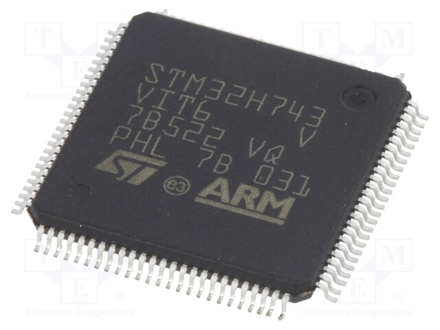
I am building a my own flight control system built around the STM32H743VIT6 (High-speed H7 architecture) , This flight controller is design for modern FPV drones. Designed on a standard 30x30mm footprint, the board focuses on zero-latency flight d…
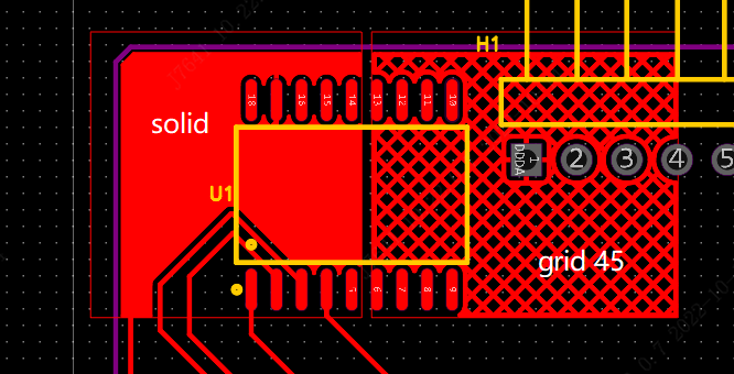
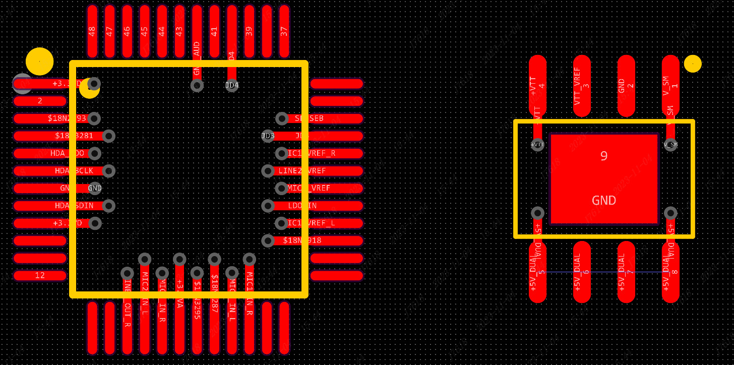
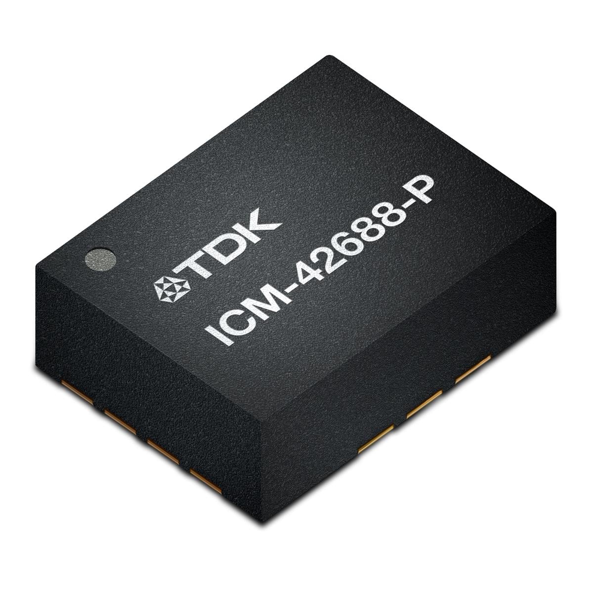
I am building a my own flight control system built around the STM32H743VIT6 (High-speed H7 architecture) , This flight controller is design for modern FPV drones. Designed on a standard 30x30mm footprint, the board focuses on zero-latency flight dynamics and crystal-clear video transmission. It features the industry-leading ICM-42688-P gyroscope on a dedicated high-speed SPI bus, and a massive 32MB onboard flash memory for flight data logging.
- STM32H743VIT6 (High-speed H7 architecture) high-performance MCU integrated as the main flight processor.
- 8MHz external resonator added for stable system timing.
- ICM-42688-PC 6-axis IMU implemented for high-precision motion tracking.
*BMP388 High-precision barometric pressure sensor - OSD: AT7456E Analog video overlay for real-time telemetry.
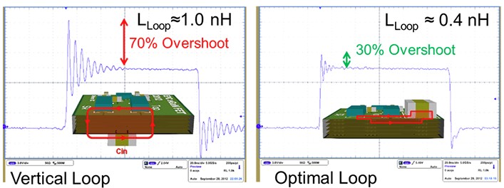
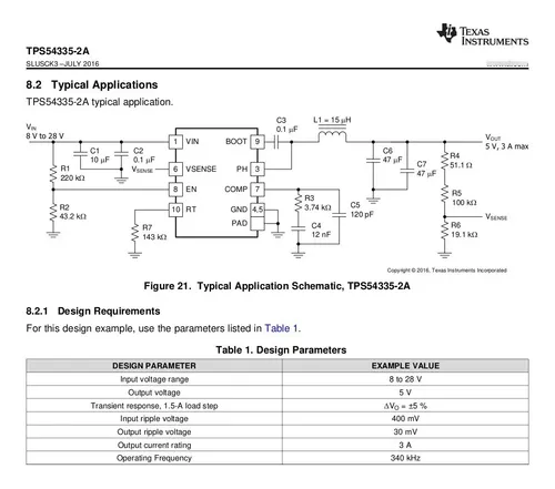
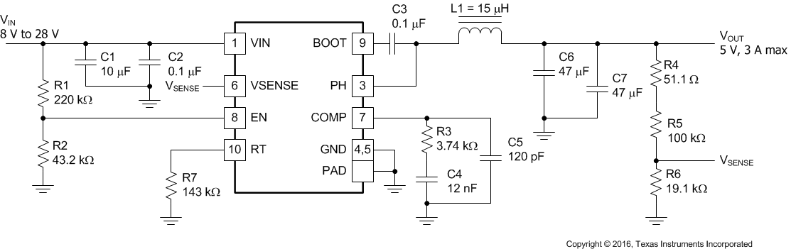
- Power System: Dual, isolated TPS54335A buck converters (5V Logic / 9V Video) with TVS spike protection.


 ,
,


.png)


