14 devlogs
25h 0m 18s
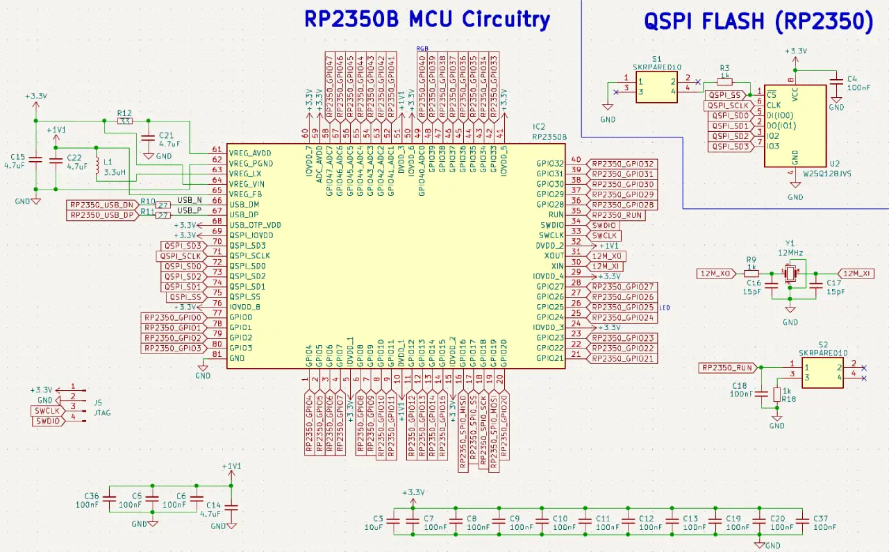
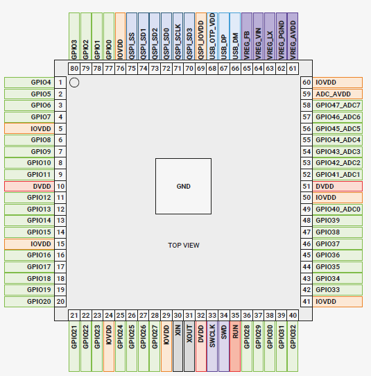
The Lemon Pi is a custom hardware development board built around RP2350B for general use case,hardware auditing, automotive testing, and computer vision projects.
It combines a powerful dual-core processor, a dedicated camera interface, and a b…
The Lemon Pi is a custom hardware development board built around RP2350B for general use case,hardware auditing, automotive testing, and computer vision projects.
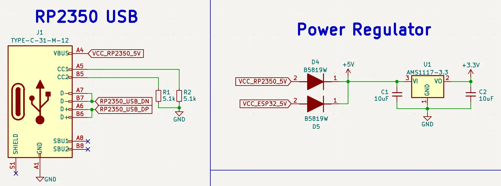
It combines a powerful dual-core processor, a dedicated camera interface, and a built-in hardware debugger. Most importantly, it features complete physical isolation between the board and your computer, protecting your laptop from dangerous voltage spikes when connecting to vehicle networks or industrial hardware.
Hardware Specifications
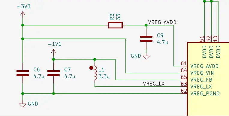
- Main Processor: Raspberry Pi RP2350B
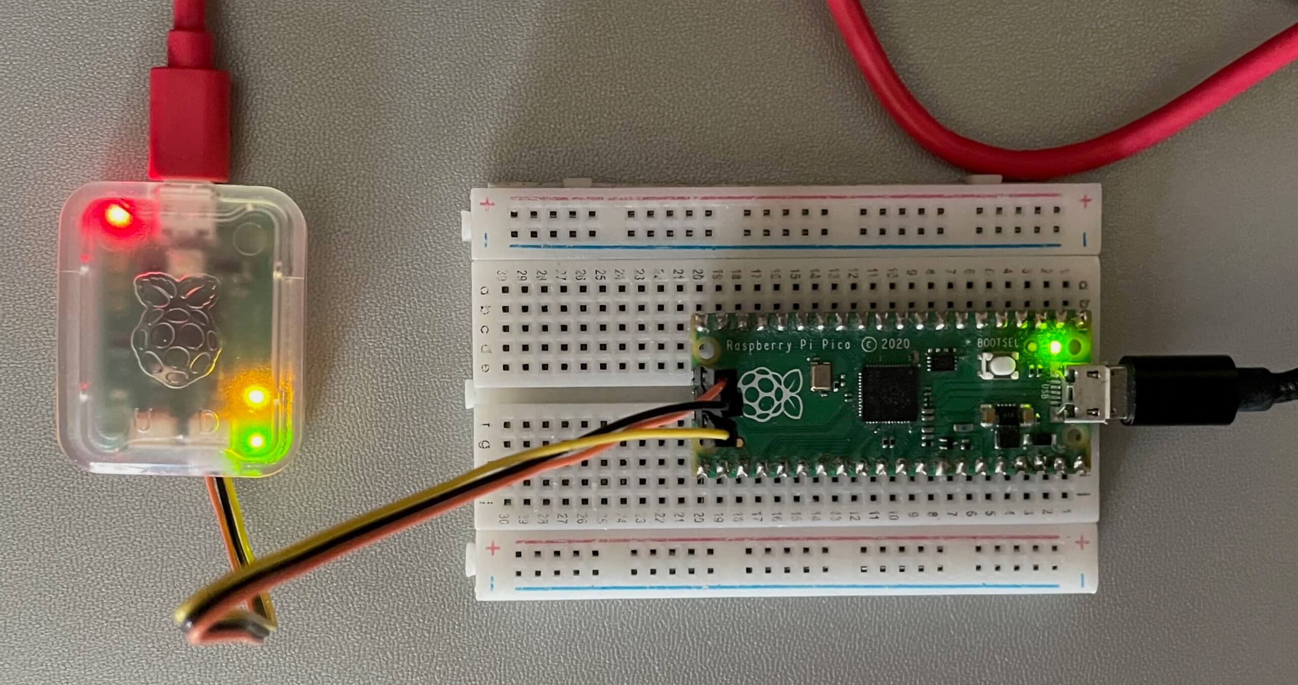
- Built-in Debugger: RP2040 acting as an onboard programmer (Picoprobe)
- Memory: 16MB Flash for firmware, plus an 8MB PSRAM
- Hardware Protection: Fully isolated USB Type-C port using ADuM3160 and B0505S chips
- Automotive: 1x CAN-FD interface with a 3-pin terminal block and selectable 120-ohm termination
- Wireless: Wi-Fi 4 and Bluetooth 5.2 built-in via the RM2 module (SPI interface)
- Vision: 24-pin DVP camera port


 )
)